A WSe2 vertical field emission transistor
 *abc
Francesca
Urban,
abc
Maurizio
Passacantando,
d
Niall
McEvoy,
e
Laura
Iemmo,
abc
Giuseppe
Luongo,
abc
Francesco
Romeo
ac
and
Filippo
Giubileo
c
*abc
Francesca
Urban,
abc
Maurizio
Passacantando,
d
Niall
McEvoy,
e
Laura
Iemmo,
abc
Giuseppe
Luongo,
abc
Francesco
Romeo
ac
and
Filippo
Giubileo
c
Abstract
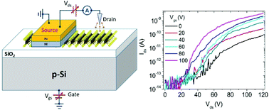
We report the first observation of a gate-controlled field emission current from a tungsten diselenide (WSe2) monolayer, synthesized by chemical-vapour deposition on a SiO2/Si substrate. Ni contacted WSe2 monolayer back-gated transistors, under high vacuum, exhibit n-type conduction and drain-bias dependent transfer characteristics, which are attributed to oxygen/water desorption and drain induced Schottky barrier lowering, respectively. The gate-tuned n-type conduction enables field emission, i.e. the extraction of electrons by quantum tunnelling, even from the flat part of the WSe2 monolayers. Electron emission occurs under an electric field ∼100 V μm−1 and exhibits good time stability. Remarkably, the field emission current can be modulated by the back-gate voltage. The first field-emission vertical transistor based on the WSe2 monolayer is thus demonstrated and can pave the way to further optimize new WSe2 based devices for use in vacuum electronics.
 Please wait while we load your content...

