
Bifacial stamping for high efficiency perovskite solar cells†

Abstract
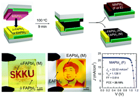
We report a novel approach for a fast phase transition of FAPbI3 (FA = formamidinium) at low-temperature and the effective removal of interfacial recombination in MAPbI3 (MA = methylammonium). This method also allows for printing (patterning) of the perovskite on a desired area. The pre-annealed MAPbI3 and δ-phase FAPbI3 films were prepared by spin-coating DMSO and a polar aprotic solvent admixed precursor solution at 65 °C and 100 °C for about 1 min, respectively, to form adduct films containing DMSO. Two films were sandwiched without pressure by a method called bifacial stamping, and annealed at 100 °C for 9 min, which resulted in complete δ → α phase transition of FAPbI3 and led to a power conversion efficiency (PCE) of 18.34%. The stamped MAPbI3 demonstrated a PCE of 20.18% that was much higher than the conventionally annealed MAPbI3 (∼17.4%) mainly due to a much higher fill factor and open-circuit voltage. Optical and structural studies revealed that DMSO-mediated ion exchange plays a vital role in the phase transition of FAPbI3 and the surface modification of MAPbI3. Theoretical calculation results further support the role of DMSO in the phase transition at low temperature. Stamping was applied to EAPbI3 (EA = ethylammonium), where photoinactive yellow EAPbI3 changed to photoactive EAPbI3 with a PCE of 13.02% after stamping with MAPbI3. The DMSO-mediated EA/MA ion exchange reaction during the stamping process created a new layer having a gradient solid solution of EAPbI3 and MAPbI3, which was responsible for the abnormally high PCE of the EAPbI3 based perovskite solar cell. Facilitated ion transport by a Lewis base (such as DMSO) reservoir in the perovskite adduct film is suggested to be involved in the bifacial stamping procedure.
 Please wait while we load your content...

