The electric field modulation of electronic properties in a type-II phosphorene/PbI2 van der Waals heterojunction†
Abstract
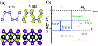
Lead iodide (PbI2), a high-quality, single-layer, large-area material, has recently been experimentally acquired in a relatively simple manner. As a layered semiconductor material with an ideal band gap, it is also an important precursor of lead halide perovskites, making it an ideal material for manufacturing the next-generation optoelectronic devices. However, at present, there have been few theoretical studies reported on PbI2. Moreover, by constructing a vertical van der Waals (vdW) heterojunction, the excellent properties of various materials can be well utilized. Therefore, the study of a two-dimensional (2D) vdW heterojunction based on phosphorene/PbI2 (P/PbI2) will be very useful. In this study, a P/PbI2 vdW heterojunction was constructed, and its electronic properties were studied using the first-principles calculations based on the density functional theory (DFT) method. The calculation result shows that the P/PbI2 vdW heterojunction has a distinct type-II band alignment, whose direct band gap value is 0.52/0.83 eV in DFT/HSE06. Moreover, the band gap of the heterojunction can be effectively modulated under the control of an electric field, and the value of the band gap can vary from 0 to 0.90/1.54 eV in DFT/HSE06. Collectively, these findings provide an effective approach for designing new PbI2-based vdW heterojunctions and adjusting the electronic properties in solar energy and optoelectronic devices.

- This article is part of the themed collection: 2019 PCCP HOT Articles


 Please wait while we load your content...