Improving pseudo-van der Waals epitaxy of self-assembled InAs nanowires on graphene via MOCVD parameter space mapping
 ab
Michael A.
Slocum,
†b
Hyun
Kum,
‡b
Thomas S.
Wilhelm,
ab
Stephen J.
Polly,
b
Seth M.
Hubbard
ab
and
Parsian K.
Mohseni
*ab
ab
Michael A.
Slocum,
†b
Hyun
Kum,
‡b
Thomas S.
Wilhelm,
ab
Stephen J.
Polly,
b
Seth M.
Hubbard
ab
and
Parsian K.
Mohseni
*ab
Abstract
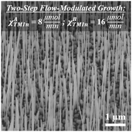
Heterogeneous self-assembly of III–V nanostructures on inert two-dimensional monolayer materials enables novel hybrid nanosystems with unique properties that can be exploited for low-cost and low-weight flexible optoelectronic and nanoelectronic device applications. Here, the pseudo-van der Waals epitaxy (vdWE) growth parameter space for heterogeneous integration of InAs nanowires (NWs) with continuous films of single layer graphene (SLG) via metalorganic chemical vapor deposition (MOCVD) is investigated. The length, diameter, and number density of NWs, as well as areal coverage of parasitic islands, are quantified as functions of key growth variables including growth temperature, V/III ratio, and total flow rate of metalorganic and hydride precursors. A compromise between self-assembly of high aspect ratio NWs comprising high number density arrays and simultaneous minimization of parasitic growth coverage is reached under a selected set of optimal growth conditions. Exploration of NW crystal structures formed under various growth conditions reveals that a characteristic polytypic and disordered lattice is invariant within the explored parameter space. A growth evolution study reveals a gradual reduction in both axial and radial growth rates within the explored timeframe for the optimal growth conditions, which is attributed to a supply-limited competitive growth regime. Two strategies are introduced for further growth optimization. Firstly, it is shown that the absence of a pre-growth in situ arsine surface treatment results in a reduction of parasitic island coverage by factor of ∼0.62, while NW aspect ratio and number densities are simultaneously enhanced. Secondly, the use of a two-step flow-modulated growth procedure allows for realization of dense fields of high aspect ratio InAs NWs. As a result of the applied studies and optimization of the growth parameter space, the highest reported axial growth rate of 840 nm min−1 and NW number density of ∼8.3 × 108 cm−2 for vdWE of high aspect ratio (>80) InAs NW arrays on graphitic surfaces are achieved. This work is intended to serve as a guide for vdWE of self-assembled III–V semiconductor NWs such as In-based ternary and quaternary alloys on functional two-dimensional monolayer materials, toward device applications in flexible optoelectronics and tandem-junction photovoltaics.
 Please wait while we load your content...

