
Novel approaches and scalability prospects of copper based hole transporting materials for planar perovskite solar cells

Abstract
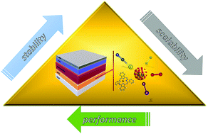
A decade after their first appearance as components of solar cells, perovskites are still at the center of solar research. Material and device engineering has led to high PCE values that now surpass 22%. Even though the lion's share is devoted to the development of perovskite structures, which has been crucial for the leap in efficiency values, the charge transport layers – electrons and holes – have a significant effect on the corresponding devices’ performance as well. The determining effect of these layers’ properties is particularly reflected in the stability of devices, especially when moving from lab scale to large scale. For the ability of PSC technology to make a step towards their commercialization, stable and low cost, large area PSCs need to be demonstrated and even though significant advances have been made in demonstrating stable modules and panels, the cost remains an inhibiting factor for potential investments in this field. Among the components of a PSC, the HTL is responsible for a great part of the cost, since the most efficient devices so far incorporate expensive HTMs, such as spiro-OMeTAD and PTAA. The inverted structure PSCs offer a wide range of alternative HTLs, since in this device configuration the HTL is deposited below the easily destructible perovskite layer. Hence, any material with modest hole mobility is a potential alternative for the replacement of the costly HTMs used so far. In this context, we have gathered the most recent works that have been demonstrated, regarding Cu based materials applied as HTMs in planar p-i-n structure PSCs. This family of materials is receiving an increasing amount of interest in the scientific community, owing to their favorable charge transfer properties (e.g. high hole mobility), their physical properties (e.g. solubility in various solvents), their ability to form dense, uniform and smooth films, with numerous methods and most importantly their low cost. We expect that this review, by presenting and discussing the applications of Cu based materials as HTMs in planar PSCs, in a clear and thorough way, will highlight their importance and capabilities in the field and provide a motivation towards their further exploration.
- This article is part of the themed collection: Recent Review Articles
 Please wait while we load your content...

