Electrical and geometrical tuning of MoS2 field effect transistors via direct nanopatterning†
 a
A.
Black,
b
Ramón
Bernardo-Gavito,
c
A. L.
Vázquez de Parga,
ad
D.
Granados
*a
a
A.
Black,
b
Ramón
Bernardo-Gavito,
c
A. L.
Vázquez de Parga,
ad
D.
Granados
*a
Abstract
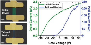
Mechanically exfoliated van der Waals materials can be used to prepare proof-of-concept electronic devices. Their optoelectronic properties strongly depend on the geometry and number of layers present in the exfoliated flake. Once the device fabrication steps have been completed, tuning the device response is complex, since the geometry and number of layers cannot be easily modified. In this work, we employ Pulsed Focused Electron Beam Induced Etching (PFEBIE) to tailor the geometry and electronic properties of field effect transistors based on mechanically exfoliated Molybdenum Disulfide (MoS2) flakes. First, MoS2 field effect transistors are fabricated via optical lithography and conventional methods. Then, the geometry of the MoS2 source–drain conduction channel is modified employing a Xenon difluoride (XeF2) gas injection nozzle combined with a pulsed electron beam pattern-generation system. Electrical characterization of devices carried out before and after the nanopatterning step via PFEBIE reveals a shift in the doping from N-type towards P-type. We attribute this change to sulfur vacancies induced during the direct nanopatterning step. This is confirmed by micro-Raman and micro-Photoluminescence spectroscopy experiments. The direct nanopatterning method allows us to fine-tune the geometry and thus the electronic properties of the devices, once the conventional fabrication steps have been completed. The success rate of our tailoring method exceeds 85% when tuning the geometry of the flake into a 250 nm wide and straight conduction channel between source and drain.
 Please wait while we load your content...

