
Location-selective growth of two-dimensional metallic/semiconducting transition metal dichalcogenide heterostructures†

Abstract
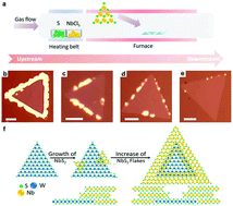
An electrical contact between metallic electrodes and semiconductors is critical for the performance of electronic and optoelectronic devices. Two-dimensional (2D) transition metal dichalcogenides (TMDs) contain semiconducting, metallic and insulating material members, which enables the fabrication of highly integrated electronic devices fully based on 2D TMDs. However, location-selective synthesis of metallic/semiconducting heterostructures by a chemical vapor deposition (CVD) method has rarely been reported. In this study, a two-step CVD method was applied to fabricate 2D metallic/semiconducting heterostructures. Semiconducting WS2 was first synthesized and served as the template for the following CVD growth of metallic NbS2. In the growth process, NbS2 flakes selectively nucleate at the edges of WS2 monolayers, thus resulting in the formation of NbS2 islands circling around the WS2 monolayers. The as-grown NbS2/WS2 heterostructure was further systematically characterized by Raman spectroscopy, atomic force microscopy (AFM) and scanning transition electron microscopy (STEM). The NbS2 layers epitaxially grown on the WS2 monolayers exhibit a 3R phase and there was no discernible lattice strain in the NbS2/WS2 van der Waals (vdW) heterostructure. The growth of the metallic/semiconducting 2D heterostructures could benefit the nanoelectronic device fabrication and provide a platform for the 2D contact resistance study.
 Please wait while we load your content...

