Additive solution deposition of multi-layered semiconducting polymer films for design of sophisticated device architectures†
Abstract
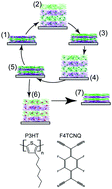
Many organic electronic devices require vertically layered structures to operate. This manuscript demonstrates an additive solution process for depositing multiple layers of semiconducting polymer (SP) films by controlling film solubility with molecular dopants. During multi-layer deposition the bottom layers are exposed to a series of solvent environments that swell the SP films. We use neutron reflectometry (NR) to quantify the film thickness change and solvent content during solvent exposure in a single poly-3-hexylthiophene (P3HT) layer. The film thickness increases by 40–80% with exposure to good solvents. Four layer thin-films composed of alternating protonated and deuterated P3HT layers were additively coated from solution. NR measurements reveal high individual layer purity and that extensive solvent soaking induces no mixing between layers. Finally, two-point conductivity measurements demonstrate that P3HT:P3HT layer interfaces have no effect on vertical conductivity. This facile process enables additive layering of mutually soluble SP films and can be used to design novel electronic device architectures.


 Please wait while we load your content...