
Anodizing with voltage versus optical path length modulation: a new tool for the preparation of photonic structures†
 *ab
Kirill S.
Napolskii
ab
*ab
Kirill S.
Napolskii
ab
Abstract
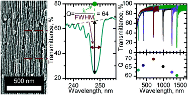
One-dimensional photonic crystals – multilayered structures with periodic modulation of a refractive index – are of great practical importance in modern materials science and nanotechnology owing to a variety of their applications in optoelectronics, solar photovoltaics, and sensorics. Anodizing of valve metals under oscillating conditions, which allows one to produce porous oxide films with modulated porosity across the film thickness, is a low-cost, scalable, and reproducible method for the preparation of 1D photonic crystals. However, precise control of the refractive index and the optical path length of the single layers in anodic oxides is still a challenge, mainly due to the chemical widening of pores in the upper part of the oxide film during the anodizing and, thus destruction of the structural periodicity produced electrochemically. Here, a novel anodizing regime with feedback, which takes into account the rate of chemical etching as a parameter, is suggested for the precise control of morphology of the porous films of anodic oxides of valve metals. The suggested approach allows one to apply anodizing voltage as a function of the optical path length of an oxide layer. The potential of the suggested approach is demonstrated by the preparation of one-dimensional anodic alumina photonic crystals with an unprecedentedly high quality factor of the photonic band gaps. The possibility to tune the position of a photonic band gap within the range of 250–1400 nm with an inaccuracy of <1% is shown.
- This article is part of the themed collection: Photonics
 Please wait while we load your content...

