Reducing the contact and channel resistances of black phosphorus via low-temperature vacuum annealing†
Abstract
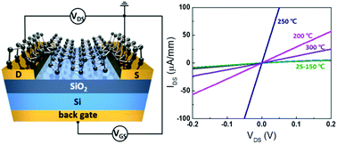
The effects of post-fabrication vacuum annealing on the performance of black phosphorus (BP) field-effect transistors (FETs) were investigated. Ohmic contact to the BP layer was improved after vacuum annealing below 250 °C, showing better linearity in current–voltage output characteristics. In addition, the channel resistance was greatly improved from 39.5 to 0.299 kΩ mm after vacuum annealing over 200 °C due to the desorption of residues and adsorbates, which led to an enhanced device performance including a higher current injection efficiency, field-effect hole mobility (5.04 to 140 cm2 V−1 s−1), current on/off ratio (2.34 to 370), lower Ohmic loss (17.8 to 0.103 kΩ mm), and less hysteresis. The field-effect hole mobilities and current on/off ratios of the BP FET device vacuum-annealed at 250 °C were found to be 28 and 158 times higher, respectively, than those of the as-fabricated device. However, the device performance deteriorated after vacuum annealing over 300 °C owing to the catalytic amorphization of BP caused by the metal electrodes. Our results pave the way towards the development of high-performance BP-based devices with minimal parasitic elements via low-temperature vacuum annealing.


 Please wait while we load your content...