Electronic band structures of undoped and P-doped Si nanocrystals embedded in SiO2
Abstract
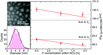
Due to their interesting optical and electronic properties, silicon nanocrystals (Si NCs) are the subject of intense research activity. The definition of their electronic structure is not trivial, neither from a theoretical nor from an experimental point of view. In fact, the models and methodologies developed for bulk materials cannot be directly applied to study these nanostructures where size-related effects, like quantum confinement (QC) and surface related phenomena, play a major role. In this work, X-ray Photoelectron Spectroscopy (XPS) was used to study the electronic structure of Si NCs embedded in SiO2. The energy differences among Si0+ 2s and Si0+ 2p core levels and the valence band maximum (VBM) were monitored. XPS data were combined with a direct measurement of the energy band gap by photoluminescence analysis, providing a complete picture of the electronic structure of Si NCs as a function of their size. Experimental data indicate a progressive reduction of energy differences among core levels and the VBM when decreasing the average diameter of the Si NCs. No concomitant shift of the conduction band minimum (CBM) was observed. The electronic structure of P-doped Si NCs was investigated as well, showing a concurrent shift of the VBM and the CBM as a function of P concentration.


 Please wait while we load your content...