
Localized effect of PbI2 excess in perovskite solar cells probed by high-resolution chemical–optoelectronic mapping†
 a
Samuele
Lilliu,
b
Vikas
Kumar,
c
Harrison Ka Hin
Lee,
a
David
Lidzey
b
and
Wing Chung
Tsoi
*a
a
Samuele
Lilliu,
b
Vikas
Kumar,
c
Harrison Ka Hin
Lee,
a
David
Lidzey
b
and
Wing Chung
Tsoi
*a
Abstract
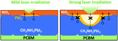
We report the laser irradiation of CH3NH3PbI3 solar cells to generate and control localized PbI2 degradation product. We show that by tuning the laser power and illumination time, we can controllably form a local excess of PbI2. High-resolution advanced multi-mapping techniques are used to highlight the effect of PbI2 on the photophysical and photoelectrical properties in a complete perovskite device. Whereas a thick PbI2 film at the perovskite/hole transport layer interface has a detrimental effect on the photocurrent and photoluminescence, a thin PbI2 film (<20 nm) leads to a significant photocurrent increase, which is ascribed to the passivation of non-radiative defects and reduced charge recombination at the interface. Our findings reveal that laser irradiation is a new approach to understand the effect of PbI2 surface layers and potentially offers a means to passivate trap states and improve PV properties of perovskite devices.
 Please wait while we load your content...

