Single-crystal-like optoelectronic-properties of MAPbI3 perovskite polycrystalline thin films†
Abstract
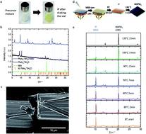
Our understanding of the crystallization process of hybrid halide perovskites has propelled the efficiency of state-of-the-art photovoltaic devices to over 22%. Further improvements to the performance will likely arise from reducing the number of grain boundaries. Here, current methods lead to grain sizes in the 1 micrometer range and the resulting optoelectronic properties suffer as compared to single-crystal materials. In this work, we introduce a new synthesis procedure with MAPbI3 leading to crystal sizes in the tens of microns range. This approach is based on the pre-crystallization of an intermediate phase (IP) based on the solid-state reaction of a lead-acetate trihydrate precursor mixture in a highly polar solvent. Beyond large grain sizes, the crystal orientation is also tightly controlled, leading to perovskite crystallites which remain perfectly aligned with the c-axis of the tetragonal structure parallel to the substrate as evidenced by grazing incidence wide angle X-ray scattering (GIWAXS). Furthermore, we demonstrate the high crystallinity and large grain size of the developed films via high-resolution transmission electron microscopy (HRTEM). The charge carrier mobilities are significantly improved with larger grain size and approach mobility values of about 40 cm2 V−1 s−1, moving toward the values observed for single crystals. We capitalize on the enhanced optoelectronic properties of the developed films by incorporating them into planar heterojunction solar cells which reach power conversion efficiencies of 18.5%, higher than MAPbI3-based device prepared from standard methods in a like-to-like comparison.


 Please wait while we load your content...