Two-dimensional black phosphorus: its fabrication, functionalization and applications
Abstract
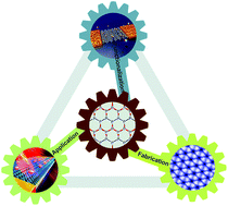
Phosphorus, one of the most abundant elements in the Earth (∼0.1%), has attracted much attention in the last five years since the rediscovery of two-dimensional (2D) black phosphorus (BP) in 2014. The successful scaling down of BP endows this ‘old material’ with new vitality, resulting from the intriguing semiconducting properties in the atomic scale limit, i.e. layer-dependent bandgap that covers from the visible light to mid-infrared light spectrum as well as hole-dominated ambipolar transport characteristics. Intensive research effort has been devoted to the fabrication, characterization, functionalization and application of BP and other phosphorus allotropes. In this review article, we summarize the fundamental properties and fabrication techniques of BP, with particular emphasis on the recent progress in molecular beam epitaxy growth of 2D phosphorus. Subsequently, we highlight recent progress in BP (opto)electronic device applications achieved via customized manipulation methods, such as interface, defect and bandgap engineering as well as forming Lego-like stacked heterostructures.

- This article is part of the themed collection: Recent Review Articles


 Please wait while we load your content...