Ultrafast interfacial transformation from 2D- to 3D-bonded structures in layered Ge–Sb–Te thin films and heterostructures†
Abstract
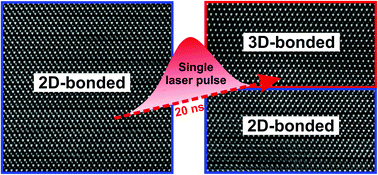
Two-dimensional van-der-Waals-bonded chalcogenide heterostructures have recently received a lot of attention due to promising applications in the fields of photonics, plasmonics and data storage. Of particular interest is the interfacial switching process inherent in these structures, which is assumed to occur locally at the van-der-Waals interfaces and thus represents an intracrystalline transition. However, detailed experimental studies on the underlying mechanism are still lacking. In this work, epitaxially grown thin films consisting of van-der-Waals-bonded Ge–Sb–Te and GeTe/Sb2Te3 based heterostructures are employed as a model system to investigate structural changes induced by a single ns-laser pulse. A combined approach using X-ray diffraction and advanced transmission electron microscopy is applied to study phase transitions within the Ge–Sb–Te-based thin films in detail. The results reveal ultrafast transitions from 2D-bonded layered structures to 3D-bonded structures via a transient molten phase. Moreover, the interface between the 2D- and 3D-bonded structures is well defined by a single van-der-Waals gap, suggesting that the transition can be controlled very precisely in its spatial extent by an appropriate choice of the laser fluence. Overall, the results of this work offer a new perspective on the switching mechanism in Ge–Sb–Te-based materials and demonstrate the potential of van-der-Waals-bonded Ge–Sb–Te compounds to be applied for novel phase-change memory concepts.


 Please wait while we load your content...