Visualizing charges accumulated in an electric double layer by three-dimensional open-loop electric potential microscopy
 *ac
*ac
Abstract
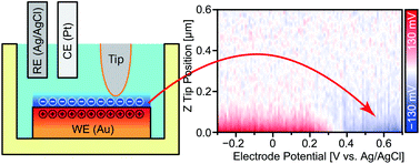
Charges accumulated in an electric double layer (EDL) play key roles in various interfacial phenomena and electronic devices. However, direct imaging of their spatial distribution has been a great challenge, which has hindered our nano-level understanding of the mechanisms of such interfacial phenomena and functions. In this study, we present direct imaging of charges accumulated at an electrode–electrolyte interface using three-dimensional open-loop electric potential microscopy (3D-OL-EPM). Conventional OL-EPM allows us to visualize two-dimensional potential distributions in liquid yet the zero of the measured potential is not well defined due to the influence of the long-range (LR) interaction between the cantilever and the sample. Here, we present practical ways to reduce such an influence by improving the equation for the potential calculation and subtracting the LR contribution estimated from a Z potential profile. These improvements enabled the calibration of the measured potential values with respect to the bulk solution potential. With these improvements, we visualized opposite charge accumulation behaviors on a polarizable and non-polarizable electrode with a varying electrode potential. Combining OL-EPM with a 3D tip scanning method, we also performed a 3D-OL-EPM measurement on a Cu fine wire and visualized the nanoscale distribution of the charges accumulated at the interface. Such real-space information on the charge distributions in an EDL should provide valuable insights into the mechanisms of interfacial phenomena and functions that are important in various academic and industrial research on electronic devices, electrochemistry, tribology and life sciences.
- This article is part of the themed collection: Industry R&D collection
 Please wait while we load your content...

