Formation of nanocrystalline graphene on germanium†
Abstract
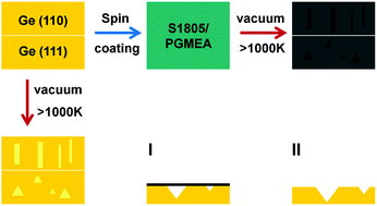
Graphitization of a polymer layer provides a convenient route to synthesize nanocrystalline graphene on dielectric surfaces. The transparent and conducting wafer scale material is of interest as a membrane and a coating, and for the generation and detection of light, or strain sensing. In this work, we study the formation of nanocrystalline graphene on germanium, a surface which promotes the CVD synthesis of monocrystalline graphene. The surprising result that we obtained through graphitization is the formation of cavities in germanium, over which nanocrystalline graphene is suspended. Depending on the crystallographic orientation of the germanium surface, either trenches in (110)–Ge or pits in (111)–Ge are formed, and their dimensions depend on the graphitization temperature. Using Raman spatial imaging, we can show that nanocrystalline graphene is formed across the entire wafer in spite of the cavity formation. Interestingly, the Raman intensity is suppressed when the material is supported by germanium and is enhanced when the material is suspended. Through simulations, we can show that these effects are induced by the high refractive index of germanium and by interferences of the light field depending on the spacing between graphene and germanium. Using atomic force and scanning electron microscopy, we determined that ripples in the suspended material are induced by the mismatch of thermal expansion coefficients. Our results provide a new route to lithography-free fabrication of suspended membranes.


 Please wait while we load your content...