Moldable biomimetic nanoscale optoelectronic platforms for simultaneous enhancement in optical absorption and charge transport†
Abstract
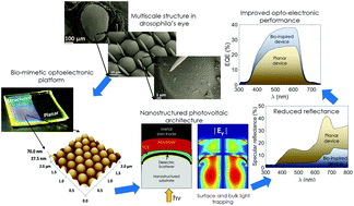
Nano-scale patterns such as those found on the exterior surface of the eyes of certain nocturnal insects have far-reaching implications in terms of optoelectronic device design. The advantage of using these patterns for optoelectronic enhancement in photovoltaic light harvesting has been less explored due to the lack of suitable engineered materials to easily fabricate such nanostructures. Here, an attempt is made to realize these complex patterns using a self-assembly based molding process on hitherto unexplored robust structural epoxies with excellent repeatability and scalability to a larger area. The incorporation of these patterns in the substrate shows nearly a 50% broadband drop in the specular reflectance of the nanostructured substrate. Furthermore, it is demonstrated that by tweaking the bio-inspired patterns on the interior side of a light harvesting device, it is possible to obtain a broadband improvement in the external quantum efficiency in the spectral window between 350 and 650 nm leading to a significant improvement of up to 49% in the photocurrent density in the structured devices. From our experiment and simulations, it is observed that this enhancement stems from a combination of two effects: first, a broadband drop in the specular reflectance exceeding 70%, arising from trapped surface plasmon-polariton modes, and second, an improved charge separation in the structured device arising due to perturbed built-in electric fields. Furthermore, the simulations which take into account the interfacial nano-scale morphology show that for absorbers with low carrier mobilities, a significant improvement in the photocurrent and in the fill factor is simultaneously possible. Overall, this work demonstrates a combination of tweaked bio-mimetic design and the use of unconventional robust structural materials as nanostructured optoelectronic substrates. This effort can bridge the gap between naturally evolved designs and practical optoelectronics to enhance the performance.


 Please wait while we load your content...