
Fabrication of a solution-processed, highly flexible few layer MoS2 (n)–CuO (p) piezotronic diode on a paper substrate for an active analog frequency modulator and enhanced broadband photodetector†

Abstract
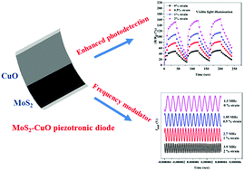
In this work, we demonstrate for the first time, a solution-processed MoS2 (n)–CuO (p) piezotronic diode on a flexible paper substrate for an enhanced broadband photodetector and active analog frequency modulator by application of external mechanical strain. There are no reports on solution-processed large area fabrication of MoS2-based heterojunctions wherein the external mechanical strain modulates the transport properties at the device level which can be further utilized at the circuit level for frequency modulation. When external strain is applied, because of the non-centrosymmetric structure of MoS2, the piezopotential induced adjusts the band structure at the junction and broadens the depletion region, which decreases the depletion capacitance of the diode. The widening of the depletion region improves the separation of photo-generated carriers and enhances the performance of the diode under both visible and NIR illumination. The fabricated piezotronic diode exhibited higher responsivity towards visible light illumination when compared to NIR illumination. The responsivity of the fabricated piezotronic diode increased by 69.7% under 2% strain. Such a versatile technique for fabrication of a diode and its utilization at both the device and circuit levels is a major step ahead in flexible and wearable electronics with applications ranging from digital, to analog, and optoelectronics.
 Please wait while we load your content...

