Issue 1, 2017

The impact of post-deposition annealing on the performance of solution-processed single layer In2O3 and isotype In2O3/ZnO heterojunction transistors

Abstract

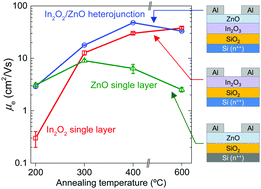
We study the influence of post-deposition annealing temperature on the morphology, chemical state and electrical properties of solution-processed single layer In2O3 and isotype In2O3/ZnO heterojunction transistors. Through careful optimisation of the material deposition and annealing conditions we demonstrate remarkable enhancement in the electron mobility of In2O3/ZnO heterojunction transistors, as compared to single layer In2O3 devices, with a maximum value of 48 cm2 V−1 s−1.

Graphical abstract: The impact of post-deposition annealing on the performance of solution-processed single layer In2O3 and isotype In2O3/ZnO heterojunction transistors

Supplementary files

Article information

Article type
Communication
Submitted
10 Nov 2016
Accepted
06 Dec 2016
First published
15 Dec 2016

J. Mater. Chem. C, 2017,5, 59-64

The impact of post-deposition annealing on the performance of solution-processed single layer In2O3 and isotype In2O3/ZnO heterojunction transistors

K. Tetzner, I. Isakov, A. Regoutz, D. J. Payne and T. D. Anthopoulos, J. Mater. Chem. C, 2017, 5, 59 DOI: 10.1039/C6TC04907A

To request permission to reproduce material from this article, please go to the Copyright Clearance Center request page.

If you are an author contributing to an RSC publication, you do not need to request permission provided correct acknowledgement is given.

If you are the author of this article, you do not need to request permission to reproduce figures and diagrams provided correct acknowledgement is given. If you want to reproduce the whole article in a third-party publication (excluding your thesis/dissertation for which permission is not required) please go to the Copyright Clearance Center request page.

Read more about how to correctly acknowledge RSC content.

Social activity

Spotlight

Advertisements