Understanding surface chemistry during MAPbI3 spray deposition and its effect on photovoltaic performance†
Abstract
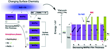
In recent years there has been significant research into organic–inorganic halide perovskites for photovoltaic applications and has resulted in power conversion efficiencies greater than 20%. A number of deposition techniques have been utilized to produce high quality perovskite films including thermal evaporation, single and two-step spin coating and vapor assisted processes. However, these laboratory based fabrication methods are not well matched with low costing, roll to roll processing that is associated with large scale manufacture. In this work we use a low costing and rapid spray coating technique to fabricate solution processed MAPbI3 films with controlled film thickness achieved through modifying concentration/spray volume. Investigation into the chemical composition and film morphology showed differing surface chemistries for the different film thicknesses, altering the surface morphology from large micro grained structures to small distorted grain arrangements. We have then implemented spray deposited films into solar devices (ITO/TiO2/MAPbI3/Au) and have studied the current density–voltage (JV) characteristics including light soaking effects. Through optimizing the absorber thickness the short-circuit current density is increased from 4.9 mA cm−2 to 22.3 mA cm−2, increasing overall power conversion efficiency by a factor >5. Investigation into the performance of devices under continued illumination showed an inverse relationship existed between low efficiency (thick) MAPbI3 films and high efficiency (thin) MAPbI3 films, where the former displayed large increases in overall performance compared to the rapid degradation in the latter. We attribute device instabilities to the increase in defect density as a consequence of the spray-induced surface chemistry, leading to trap assisted recombination at the back electrode.


 Please wait while we load your content...