Thin film transistors based on two dimensional graphene and graphene/semiconductor heterojunctions
Abstract
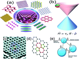
During the past few years, two-dimensional (2D) layered materials have emerged as the most fundamental building blocks of a wide variety of optoelectronic devices. The weak van der Waals (vdW) interlayer forces allow the 2D monolayers to isolate and restack into arbitrary stacking heterojunctions. The recently developed chemical vapor deposition (CVD) technique shows great promise for the production of large domain building blocks of 2D heterostructures with vertical and lateral stacking and much better device performance. This review is the first of its kind to discuss the research progress of flexible FETs based on graphene/semiconductor heterostructures, in which graphene acts as both electrode and semiconductor material.

- This article is part of the themed collections: 2017 Review articles and 2D Materials: Explorations Beyond Graphene


 Please wait while we load your content...