
Simultaneous topographical, electrical and optical microscopy of optoelectronic devices at the nanoscale†
 b
b
Abstract
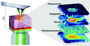
Novel optoelectronic devices rely on complex nanomaterial systems where the nanoscale morphology and local chemical composition are critical to performance. However, the lack of analytical techniques that can directly probe these structure–property relationships at the nanoscale presents a major obstacle to device development. In this work, we present a novel method for non-destructive, simultaneous mapping of the morphology, chemical composition and photoelectrical properties with <20 nm spatial resolution by combining plasmonic optical signal enhancement with electrical-mode scanning probe microscopy. We demonstrate that this combined approach offers subsurface sensitivity that can be exploited to provide molecular information with a nanoscale resolution in all three spatial dimensions. By applying the technique to an organic solar cell device, we show that the inferred surface and subsurface composition distribution correlates strongly with the local photocurrent generation and explains macroscopic device performance. For instance, the direct measurement of fullerene phase purity can distinguish between high purity aggregates that lead to poor performance and lower purity aggregates (fullerene intercalated with polymer) that result in strong photocurrent generation and collection. We show that the reliable determination of the structure–property relationship at the nanoscale can remove ambiguity from macroscopic device data and support the identification of the best routes for device optimisation. The multi-parameter measurement approach demonstrated herein is expected to play a significant role in guiding the rational design of nanomaterial-based optoelectronic devices, by opening a new realm of possibilities for advanced investigation via the combination of nanoscale optical spectroscopy with a whole range of scanning probe microscopy modes.
 Please wait while we load your content...

