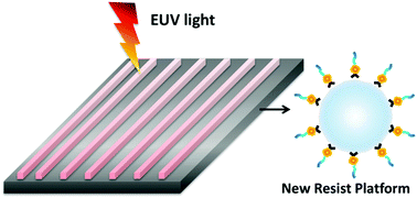
Extreme ultraviolet resist materials for sub-7 nm patterning
 *a
Shulan
Wang,
b
*a
Shulan
Wang,
b
Abstract
Continuous ongoing development of dense integrated circuits requires significant advancements in nanoscale patterning technology. As a key process in semiconductor high volume manufacturing (HVM), high resolution lithography is crucial in keeping with Moore's law. Currently, lithography technology for the sub-7 nm node and beyond has been actively investigated approaching atomic level patterning. EUV technology is now considered to be a potential alternative to HVM for replacing in some cases ArF immersion technology combined with multi-patterning. Development of innovative resist materials will be required to improve advanced fabrication strategies. In this article, advancements in novel resist materials are reviewed to identify design criteria for establishment of a next generation resist platform. Development strategies and the challenges in next generation resist materials are summarized and discussed.
 Please wait while we load your content...

