Electronic and optical properties of nanostructured MoS2 materials: influence of reduced spatial dimensions and edge effects†
Abstract
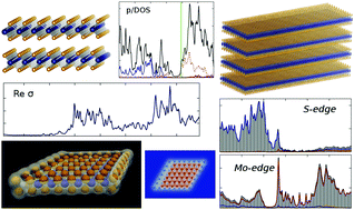
We theoretically study the electronic and optical properties of nanostructured MoS2 systems focusing on the influence of reduced spatial dimensions and edge effects, which lead to the change in character from semiconducting to metallic. For nanowires, we identify edge types which lead to the creation of a bandgap, reflecting the effect of confinement: with increasing the size of the wire in lateral direction and/or number of MoS2 layers, the gap reduces. For nanodisks, we identify features in electronic properties that are universal; specifically, our calculations reveal presence of a local maximum in electronic density of states, insensitive on nanodisk's geometrical properties. By manipulating with sulfur and molybdenum atoms at the edges we tune position of Fermi energy with respect to the local maximum. We discuss total electronic density and partial electronic density for energy levels below Fermi energy, that could be used for mapping to STM images under negative bias. Our findings are extracted from a tight-binding (TB) model that includes non-orthogonal sp3d5 orbitals and spin–orbit coupling. We benchmark our TB model by comparing our results to those extracted from density functional theory and quasiparticle self-consistent GW, test different TB parameter sets, establishing the range of their validity, and discuss limitations of our model.


 Please wait while we load your content...