Simultaneous observation of surface- and edge-states of a 2D topological insulator through scanning tunneling spectroscopy and differential conductance imaging†
Abstract
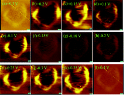
A 2D form of Bi2Se3 which acts as a topological insulator was grown through colloidal synthesis method. The surface-states and edge-states of the nanoplates were simultaneously probed through scanning tunneling spectroscopy (STS). At the interior, density of states (DOS) revealed the location of conduction and valence band edges. The DOS at the edges, on the other hand, brought out gapless conducting states along with a Dirac point at a non-zero value below the Fermi energy representing the Dirac cone of a 2D topological insulator. In differential tunnel conductance (dI/dV), images are recorded at different voltages and the two sections of the topological insulator can be viewed selectively or simultaneously with a clear contrast in illumination. Upon increasing the 2D-nanoplates thickness, the material turned into a 3D topological insulator with gapless surface states.


 Please wait while we load your content...