Epitaxial chemical vapour deposition growth of monolayer hexagonal boron nitride on a Cu(111)/sapphire substrate†
Abstract
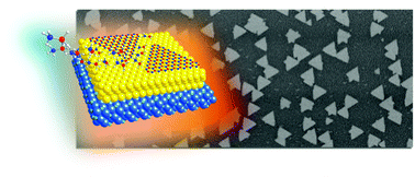
Hexagonal boron nitride (h-BN), an atomically thin insulating material, shows a large band gap, mechanical flexibility, and optical transparency. It can be stacked with other two-dimensional (2D) materials through van der Waals interactions to form layered heterostructures. These properties promise its application as an insulating layer of novel 2D electronic devices due to its atomically smooth surface with a large band gap. Herein, we demonstrated the ambient-pressure chemical vapour deposition (CVD) growth of high-quality, large-area monolayer h-BN on a Cu(111) thin film deposited on a c-plane sapphire using ammonia borane (BH3NH3) as the feedstock. Highly oriented triangular h-BN grains grow on Cu(111), which finally coalescence to cover the entire Cu surface. Low-energy electron diffraction (LEED) measurements indicated that the hexagonal lattice of the monolayer h-BN is well-oriented along the underlying Cu(111) lattice, thus implying the epitaxial growth of h-BN, which can be applied in various 2D electronic devices.


 Please wait while we load your content...