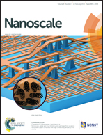
Fundamentals of lateral and vertical heterojunctions of atomically thin materials
Abstract
At the turn of this century, Herbert Kroemer, the 2000 Nobel Prize winner in Physics, famously commented that “the interface is the device”. This statement has since opened up unparalleled opportunities at the interface of conventional three-dimensional (3D) materials (H. Kroemer, Quasi-Electric and Quasi-Magnetic Fields in Non-Uniform Semiconductors, RCA Rev., 1957, 18, 332–342). More than a decade later, Sir Andre Geim and Irina Grigorieva presented their views on 2D heterojunctions which further cultivated broad interests in the 2D materials field. Currently, advances in two-dimensional (2D) materials enable us to deposit layered materials that are only one or few unit-cells in thickness to construct sharp in-plane and out-of-plane interfaces between dissimilar materials, and to be able to fabricate novel devices using these cutting-edge techniques. The interface alone, which traditionally dominated overall device performance, thus has now become the device itself. Fueled by recent progress in atomically thin materials, we are now at the ultimate limit of interface physics, which brings to us new and exciting opportunities, with equally demanding challenges. This paper endeavors to provide stalwarts and newcomers a perspective on recent advances in synthesis, fundamentals, applications, and future prospects of a large variety of heterojunctions of atomically thin materials.


 Please wait while we load your content...