Fabrication of perovskite films using an electrostatic assisted spray technique: the effect of the electric field on morphology, crystallinity and solar cell performance†
Abstract
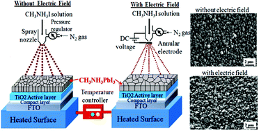
An electric field assisted spray deposition method is employed for improving the perovskite film morphology, crystallinity, and surface coverage, and for further fabricating an efficient solar cell. By applying different voltages ranging from 0.5 to 2.0 kV during spray deposition, we observed a large variation in the film morphology and surface coverage compared to those fabricated without an electric field, which is due to improved atomization from the Coulomb fission process. The optimized applied voltage of 1.5 kV during spraying led to completion of the reaction between CH3NH3I and PbI2 on a hot substrate for pure phase CH3NH3PbI3 thin film formation with improved grain growth and surface coverage. The cells fabricated using perovskite films showed clear applied voltage dependence in the energy conversion process and alleviation in J–V hysteresis; with 1.5 kV applied voltage the average cell efficiency of 8.9% was obtained compared to films fabricated without applying voltage providing only 6.5%. The best efficiencies are 10.9% and 7.37% for applied voltages of 1.5 kV and 0 kV, respectively. The enhancement in efficiency with applied voltage is due to the formation of more uniform and dense films with large perovskite crystals, which resulted in efficient electron transportation (enhanced photocurrent and modified series and shunt resistances) by minimizing the charge carrier recombination at grain boundaries (resulting in enhanced open circuit voltage). With further optimization of the perovskite film thickness by adjusting the CH3NH3I spray volume, the average cell efficiency of ∼11.0% was obtained.


 Please wait while we load your content...