Nano-scale, planar and multi-tiered current pathways from a carbon nanotube–copper composite with high conductivity, ampacity and stability
Abstract
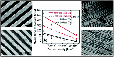
New lithographically processable materials with high ampacity are in demand to meet the increasing requirement for high operational current density at high temperatures existing in current pathways within electronic devices. To meet this demand, we report an approach to fabricate a high ampacity (∼100 times higher than Cu) carbon nanotube–copper (CNT–Cu) composite into a variety of complex nano-scale, planar and multi-tiered current pathways. The approach involved the use of a two-stage electrodeposition of copper into a pre-patterned template of porous, thin CNT sheets acting as the electrode. The versatility of this approach enabled the realization of completely suspended multi-tier, dielectric-less ‘air-gap’ CNT–Cu circuits that could be electrically isolated from each other and are challenging to fabricate with pure Cu or any metal. Importantly, all such complex structures, ranging from 500 nm to 20 μm in width, exhibited ∼100-times higher ampacity than any known metal, with comparable electrical conductivity as Cu. In addition, CNT–Cu structures also exhibited a superior temperature stability compared to the ∼10-times wider Cu counterparts. We believe that the combination of our approach and the properties demonstrated here are vital achievements for the future development of efficient and powerful electrical devices.


 Please wait while we load your content...