Novel in situ self-separation of a 2 in. free-standing m-plane GaN wafer from an m-plane sapphire substrate by HCl chemical reaction etching in hydride vapor-phase epitaxy
Abstract
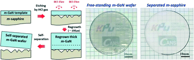
A 2 in.-diameter free-standing m-plane GaN wafer was fabricated through in situ self-separation using HCl chemical reaction etching (HCRE) in hydride vapor-phase epitaxy (HVPE). A 2 μm-thick m-plane GaN layer was directly grown on m-plane sapphire, followed by HCRE to form multiple voids at the interface between the m-plane sapphire and m-plane GaN. Void formation was attributed to preferential etching at high-defect regions (HDRs) such as stacking faults (SFs) and threading dislocations (TDs) in the m-plane GaN layer. After regrowth of an approximately 200 μm-thick m-plane GaN layer, self-separation was achieved during the cooling process. The free-standing m-plane GaN wafer was almost crack-free as a result of strain relief by the in situ self-separation process, which was confirmed by room-temperature Raman and photoluminescence measurements. It is supposed that the novel HCRE process can be applied to fabricate high-quality free-standing non-polar GaN wafers in the future.
 Please wait while we load your content...

