Effect of precursor concentration on the properties and tuning of conductivity between p-type and n-type Cu1−XCdXS2 thin films deposited by a single step solution process as a novel material for photovoltaic applications
Abstract
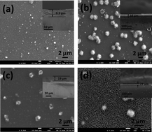
Cu1−XCdXS2 thin films were deposited from precursor solutions having different concentrations of cation sources, by a single step solution process at room temperature. The colours of the deposited films changed from light to dark brown based on the incorporation of copper and cadmium ions from the precursors. Cu1−XCdXS2 polycrystalline thin films exhibit a hexagonal structure. Cd rich films showed a sheet like morphology and poor adhesiveness owing to a cluster growth process. Wider absorption in the region 300–1300 nm was observed with a red shift in the absorption edge as the composition of Cd increased. A relative increase in the Cd composition of deposited Cu1−XCdXS2 thin films was observed as the precursor concentration of Cd increased. XPS and Raman spectra confirmed the formation of a CuCdS2 compound. Electrical properties showed the decrease in carrier concentration as Cd composition increases. The Cu1−XCdXS2 thin films exhibited both p and n-type conductivity owing to different stoichiometric ratios of cations. The analyses revealed that the Cu1−XCdXS2 thin film can be used as both a novel absorber and window layer for the fabrication of low cost thin film solar cells.
 Please wait while we load your content...

