Lateral graphene p–n junctions formed by the graphene/MoS2 hybrid interface†
Abstract
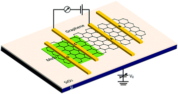
Graphene/two-dimensional (2D) semiconductor heterostructures have been demonstrated to possess many advantages for electronic and optoelectronic devices. However, there are few reports about the utilization of a 2D semiconductor monolayer to tune the properties of graphene. Here, we report the fabrication and characterization of graphene p–n junctions based on graphene/MoS2 hybrid interfaces. Monolayered graphene across the monolayered MoS2 boundary is divided into n-type regions on the MoS2 and p-type regions on the SiO2 substrate. Such van der Waals heterostructure based graphene p–n junctions show good photoelectric properties. The photocurrent modulation of such devices by a single back gate is also demonstrated for the first time, which shows that the graphene on and off MoS2 regions have different responses to the gate voltage. Our results suggest that the atomic thin hybrid structure can remarkably extend the device applications.


 Please wait while we load your content...