
Large-area synthesis of monolayer WS2 and its ambient-sensitive photo-detecting performance†
Abstract
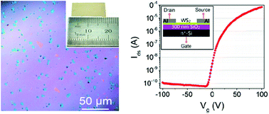
We demonstrate the synthesis of large-area monolayer WS2 films by chemical vapor deposition (CVD) and investigate their photoresponse properties by fabricating n-type field effect transistors (FETs) with Al as the ohmic contact. Our CVD-grown monolayer WS2 shows an electron mobility of 0.91 cm2 V−1 s−1 and an ON/OFF ratio of 106, indicating its comparable electronic properties to the mechanically exfoliated flake sample. In a vacuum, by applying a gate bias (60 V), the responsivity of the monolayer WS2 phototransistor can increase up to 18.8 mA W−1 and a decent sub-second level response time can be maintained. In contrast, in air, it shows a very fast response time of less than 4.5 ms, but at the cost of responsivity reduction to 0.2 μA W−1. Such a distinctive ambient-sensitive photo-detecting performance can be well-explained by the pronounced effect of charge-acceptor-like O2/H2O molecule adsorption/desorption on the photocarrier transport. Our CVD-grown high quality monolayer WS2 may pave the way for developing industrial-scale optoelectronic devices for photo-detecting and chemical sensing applications.
 Please wait while we load your content...

