
Trap density probing on top-gate MoS2 nanosheet field-effect transistors by photo-excited charge collection spectroscopy†
 b
b
Abstract
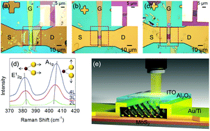
Two-dimensional (2D) molybdenum disulfide (MoS2) field-effect transistors (FETs) have been extensively studied, but most of the FETs with gate insulators have displayed negative threshold voltage values, which indicates the presence of interfacial traps both shallow and deep in energy level. Despite such interface trap issues, reports on trap densities in MoS2 are quite limited. Here, we probed top-gate MoS2 FETs with two- (2L), three- (3L), and four-layer (4L) MoS2/dielectric interfaces to quantify deep-level interface trap densities by photo-excited charge collection spectroscopy (PECCS), and reported the result that deep-level trap densities over 1012 cm−2 may exist in the interface and bulk MoS2 near the interface. Transfer curve hysteresis and PECCS measurements show that shallow traps and deep traps are not that different in density order from each other. We conclude that our PECCS analysis distinguishably provides valuable information on deep level interface/bulk trap densities in 2D-based FETs.
 Please wait while we load your content...

