Large-scale and patternable graphene: direct transformation of amorphous carbon film into graphene/graphite on insulators via Cu mediation engineering and its application to all-carbon based devices†
Abstract
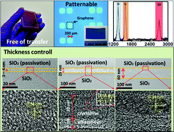
Chemical vapour deposition of graphene was the preferred way to synthesize graphene for multiple applications. However, several problems related to transfer processes, such as wrinkles, cleanness and scratches, have limited its application at the industrial scale. Intense research was triggered into developing alternative synthesis methods to directly deposit graphene on insulators at low cost with high uniformity and large area. In this work, we demonstrate a new concept to directly achieve growth of graphene on non-metal substrates. By exposing an amorphous carbon (a-C) film in Cu gaseous molecules after annealing at 850 °C, the carbon (a-C) film surprisingly undergoes a noticeable transformation to crystalline graphene. Furthermore, the thickness of graphene could be controlled, depending on the thickness of the pre-deposited a-C film. The transformation mechanism was investigated and explained in detail. This approach enables development of a one-step process to fabricate electrical devices made of all carbon material, highlighting the uniqueness of the novel approach for developing graphene electronic devices. Interestingly, the carbon electrodes made directly on the graphene layer by our approach offer a good ohmic contact compared with the Schottky barriers usually observed on graphene devices using metals as electrodes.


 Please wait while we load your content...