Layer-controlled CVD growth of large-area two-dimensional MoS2 films†
Abstract
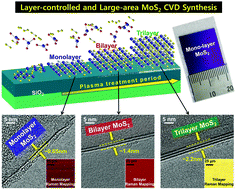
In spite of the recent heightened interest in molybdenum disulfide (MoS2) as a two-dimensional material with substantial bandgaps and reasonably high carrier mobility, a method for the layer-controlled and large-scale synthesis of high quality MoS2 films has not previously been established. Here, we demonstrate that layer-controlled and large-area CVD MoS2 films can be achieved by treating the surfaces of their bottom SiO2 substrates with the oxygen plasma process. Raman mapping, UV-Vis, and PL mapping are performed to show that mono, bi, and trilayer MoS2 films grown on the plasma treated substrates fully cover the centimeter scale substrates with a uniform thickness. Our TEM images also present the single crystalline nature of the monolayer MoS2 film and the formation of the layer-controlled bi- and tri-layer MoS2 films. Back-gated transistors fabricated on these MoS2 films are found to exhibit the high current on/off ratio of ∼106 and high mobility values of 3.6 cm2 V−1 s−1 (monolayer), 8.2 cm2 V−1 s−1 (bilayer), and 15.6 cm2 V−1 s−1 (trilayer). Our results are expected to have a significant impact on further studies of the MoS2 growth mechanism as well as on the scaled layer-controlled production of high quality MoS2 films for a wide range of applications.
 Please wait while we load your content...

