Solar energy conversion properties and defect physics of ZnSiP2†
Abstract
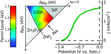
Implementation of an optically active material on silicon has been a persistent technological challenge. For tandem photovoltaics using a Si bottom cell, as well as for other optoelectronic applications, there has been a longstanding need for optically active, wide band gap materials that can be integrated with Si. ZnSiP2 is a stable, wide band gap (2.1 eV) material that is lattice matched with silicon and comprised of inexpensive elements. As we show in this paper, it is also a defect-tolerant material. Here, we report the first ZnSiP2 photovoltaic device. We show that ZnSiP2 has excellent photoresponse and high open circuit voltage of 1.3 V, as measured in a photoelectrochemical configuration. The high voltage and low band gap-voltage offset are on par with much more mature wide band gap III–V materials. Photoluminescence data combined with theoretical defect calculations illuminate the defect physics underlying this high voltage, showing that the intrinsic defects in ZnSiP2 are shallow and the minority carrier lifetime is 7 ns. These favorable results encourage the development of ZnSiP2 and related materials as photovoltaic absorber materials.


 Please wait while we load your content...