A facile room temperature iodination route to in situ fabrication of patterned copper-iodide/silicon quasi-bulk-heterojunction thin films for photovoltaic application†
Abstract
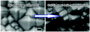
Fabrication of a monocrystalline silicon based heterojunction film at room-temperature in a time-efficient manner is desirable for energy and environmental considerations. In this report, a gas–solid phase direct elemental reaction (DER) route to realize this aim by firstly depositing an elemental copper layer on a monocrystalline silicon surface followed by a reaction with iodine vapor is described. The samples were characterized by X-ray diffraction (XRD), scanning electron microscopy (SEM), transmission electron microscopy (TEM), Raman spectroscopy, photoelectrochemical measurements, and the transient photovoltage (TPV) technique. The novelty of the current work lies in the following three aspects: (1) formation of an in situ CuI/Si quasi-bulk-heterojunction at room temperature is assisted by the infiltrated elemental copper layer being completely transformed into a γ phase copper iodide (γ-CuI) thin film; (2) the virgin monocrystalline silicon is pretreated to ensure a pyramidally patterned rough surface which facilitates the construction of quasi-bulk-heterojunction thin films and enhances their chemical stability and mechanical stability; (3) the photovoltaic performance and mechanism of the resulting CuI/Si quasi-bulk-heterojunction based solar cell was detected and evaluated for the first time by a combination of photoelectrochemical and TPV techniques, which demonstrates that the intensity of the interface electric field as well as the open circuit potential can be adjusted by tuning the amount of CuI coated on the pyramidally patterned n-Si substrate.
 Please wait while we load your content...

