Access resistance reduction in Ge nanowires and substrates based on non-destructive gas-source dopant in-diffusion
Abstract
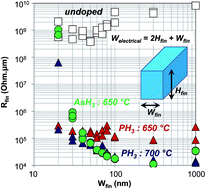
To maintain semiconductor device scaling, in recent years industry has been forced to move from planar to non-planar device architectures. This alone has created the need to develop a radically new, non-destructive method for doping. Doping alters the electrical properties of a semiconductor, related to the access resistance. Low access resistance is necessary for high performance technology and reduced power consumption. In this work the authors reduced access resistance in top–down patterned Ge nanowires and Ge substrates by a non-destructive dopant in-diffusion process. Furthermore, an innovative electrical characterisation methodology is developed for nanowire and fin-based test structures to extract important parameters that are related to access resistance such as nanowire resistivity, sheet resistance, and active doping levels. Phosphine or arsine was flowed in a Metalorganic Vapour Phase Epitaxy reactor over heated Ge samples in the range of 650–700 °C. Dopants were incorporated and activated in this single step. No Ge growth accompanied this process. Active doping levels were determined by electrochemical capacitance–voltage free carrier profiling to be in the range of 1019 cm−3. The nanowires were patterned in an array of widths from 20–1000 nm. Cross-sectional Transmission Electron Microscopy of the doped nanowires showed minimal crystal damage. Electrical characterisation of the Ge nanowires was performed to contrast doping activation in thin-body structures with that in bulk substrates. Despite the high As dose incorporation on unpatterned samples, the nanowire analysis determined that the P-based process was the better choice for scaled features.


 Please wait while we load your content...