Manipulating charge transport in a π-stacked polymer through silicon incorporation†
Abstract
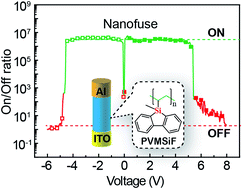
Given the fundamental importance in charge transport engineering for device operation in molecular electronics, manipulating strategies and material design principles for desired applications are highly anticipated. In stark contrast to conventional organic electronic devices, designing organic semiconductors that perform effectively as molecular nanofuses remains a challenge. Based on a novel silicon-containing π-stacked polymer of silafluorene (PVMSiF), we have successfully fabricated a molecular nanofuse device with a high ON–OFF ratio of up to 4 × 10⁶ for the first time. Using a combination of absorption and photoluminescence (PL) spectra, X-ray diffraction (XRD), micro-PL analysis supported by theoretical insights into unit and backbone geometries and wave function delocalizations provided by density functional theory (DFT) and molecular dynamics (MD) simulations, we have demonstrated the fundamental correlation between the polymer structures and the spectacular fuse-like resistive switching behaviors. It was shown that the manipulation of charge transport in π-stacked polymers is possible via silicon incorporation; molecular nanofuse devices based on π-stacked polymers can be realized following a silicon-stimulated filament mechanism with breakable π–π stacking at the charged states. These findings may have important consequences on future material studies and device applications.


 Please wait while we load your content...