Determination of Ga auto-incorporation in nominal InAlN epilayers grown by MOCVD
Abstract
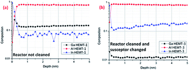
We report on the consistent measurement of gallium incorporation in nominal InAlN layers using various complimentary techniques, underpinned by X-ray diffraction. Nominal InAlN layers with similar growth conditions were prepared, and the change in unintended Ga content in the group III sublattice ranged from ∼24% to ∼12% when the total reactor flow rate was increased from 8000 to 24 000 standard cubic centimetres per minute. Ultra-thin InAlN/GaN HEMT layers were grown in a clean reactor to minimize Ga auto-incorporation, and measured using X-ray photoelectron spectroscopy and secondary ion mass spectrometry. The implications of Ga incorporation in InAlN layers within optoelectronic and power devices is discussed.


 Please wait while we load your content...