Recent advances in the growth of germanium nanowires: synthesis, growth dynamics and morphology control
Abstract
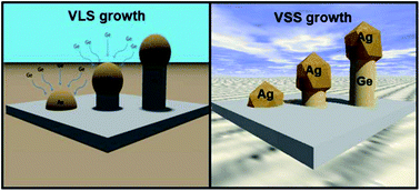
One-dimensional semiconductor nanostructures have been studied in great depth over the past number of decades as potential building blocks in electronic, thermoelectric, optoelectronic, photovoltaic and battery devices. Silicon has been the material of choice in several industries, in particular the semiconductor industry, for the last few decades due to its stable oxide and well documented properties. Recently however, Ge has been proposed as a candidate to replace Si in microelectronic devices due to its high charge carrier mobilities. A number of various ‘bottom-up’ synthetic methodologies have been employed to grow Ge nanowires, including chemical vapour deposition, thermal evaporation, template methods, supercritical fluid synthesis, molecular beam epitaxy and solution phase synthesis. These bottom-up methods afford the opportunity to produce commercial scale quantities of nanowires with controllable lengths, diameters and crystal structure. An understanding of the vapour–liquid–solid (VLS) and vapour–solid–solid (VSS) mechanism by which most Ge nanowires are produced, is key to controlling their growth rate, aspect ratio and morphology. This article highlights the various bottom-up growth methods that have been used to synthesise Ge nanowires over the past 5–6 years, with particular emphasis on the Au/Ge eutectic system and the VLS mechanism. Thermodynamic and kinetic models used to describe Ge nanowire growth and morphology control will also be discussed in detail.


 Please wait while we load your content...