Structure and transport properties of the interface between CVD-grown graphene domains†
Abstract
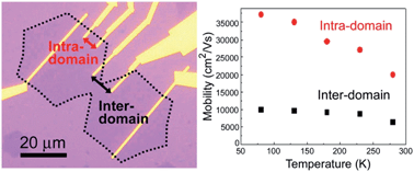
During the chemical vapor deposition (CVD) growth of graphene, graphene domains grown on a Cu surface merge together and form a uniform graphene sheet. For high-performance electronics and other applications, it is important to understand the interfacial structure of the merged domains, as well as their influence on the physical properties of graphene. We synthesized large hexagonal graphene domains with controlled orientations on a heteroepitaxial Cu film and studied the structure and properties of the interfaces between the domains mainly merged with the same angle. Although the merged domains have various interfaces with/without wrinkles and/or increased defect-related Raman D-band intensity, the intra-domain transport showed higher carrier mobility reaching 20 000 cm2 V−1 s−1 on SiO2 at 280 K (the mean value was 7200 cm2 V−1 s−1) than that measured for inter-domain areas, 6400 cm2 V−1 s−1 (mean value 2000 cm2 V−1 s−1). The temperature dependence of the mobility suggests that impurity scattering dominates at the interface even for the merged domains with the same orientation. This study highlights the importance of domain interfaces, especially on the carrier transport properties, in CVD-grown graphene.


 Please wait while we load your content...