Interface properties of CVD grown graphene transferred onto MoS2(0001)†
Abstract
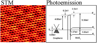
Heterostructures of dissimilar 2D materials are potential building blocks for novel materials and may enable the formation of new (photo)electronic device architectures. Previous work mainly focused on supporting graphene on insulating wide-band gap materials, such as hex-BN and mica. Here we investigate the interface between zero-band gap semiconductor graphene and band-gap semiconductor MoS2 as a potential building block for entirely 2D-material based semiconducting devices. We show that solution transfer results in water trapping at the interface which may be removed by annealing to ∼300 °C in a vacuum. After removal of the water, by high temperature annealing, ultraflat graphene is obtained on MoS2 with only a very weak moiré pattern observable in scanning tunneling microscopy images due to lattice mismatch and random alignment of graphene with respect to the MoS2 substrate. Photoemission spectroscopy indicates interface dipole formation, p-type doping of graphene by ∼0.09 eV downward shift of the Fermi-level below the Dirac point, and a negative space charge region in bulk MoS2. Interestingly, valence band spectra of the graphene covered MoS2 surface indicate a band gap narrowing of the MoS2 surface by ∼0.1 eV. This band gap reduction at the surface is further evidence that interlayer van der Waals interactions critically influence the band structure of 2D-layered dichalcogenides and suggest that interfacing with dissimilar van der Waals materials allows tuning of their electronic properties.


 Please wait while we load your content...