Issue 27, 2014

Electrical and optical characterization of atomically thin WS2

Abstract

Atomically thin layers of materials, which are just a few atoms in thickness, present an attractive option for future electronic devices. Herein we characterize, optically and electronically, atomically thin tungsten disulphide (WS2), a layered semiconductor. We provide the distinctive Raman and photoluminescence signatures for single layers, and prepare field-effect transistors where atomically thin WS2 serves as the conductive channel. The transistors present mobilities μ = 10 cm2 V−1 s−1 and exhibit ON/OFF ratios exceeding 100 000. Our results show that WS2 is an attractive option for applications in electronic and optoelectronic devices and pave the way for further studies in this two-dimensional material.
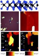
Graphical abstract: Electrical and optical characterization of atomically thin WS2

Article information

Article type
Communication
Submitted
27 Aug 2013
Accepted
24 Sep 2013
First published
27 Sep 2013

Dalton Trans., 2014,43, 10388-10391

Electrical and optical characterization of atomically thin WS2

T. Georgiou, H. Yang, R. Jalil, J. Chapman, K. S. Novoselov and A. Mishchenko, Dalton Trans., 2014, 43, 10388 DOI: 10.1039/C3DT52353E

To request permission to reproduce material from this article, please go to the Copyright Clearance Center request page.

If you are an author contributing to an RSC publication, you do not need to request permission provided correct acknowledgement is given.

If you are the author of this article, you do not need to request permission to reproduce figures and diagrams provided correct acknowledgement is given. If you want to reproduce the whole article in a third-party publication (excluding your thesis/dissertation for which permission is not required) please go to the Copyright Clearance Center request page.

Read more about how to correctly acknowledge RSC content.

Social activity

Spotlight

Advertisements