
Hybrid pn-junction solar cells based on layers of inorganic nanocrystals and organic semiconductors: optimization of layer thickness by considering the width of the depletion region
Abstract
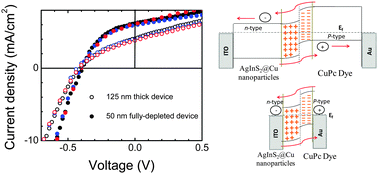
We report the formation and characterization of hybrid pn-junction solar cells based on a layer of copper diffused silver indium disulfide (AgInS2@Cu) nanoparticles and another layer of copper phthalocyanine (CuPc) molecules. With copper diffusion in the nanocrystals, their optical absorption and hence the activity of the hybrid pn-junction solar cells was extended towards the near-IR region. To decrease the particle-to-particle separation for improved carrier transport through the inorganic layer, we replaced the long-chain ligands of copper-diffused nanocrystals in each monolayer with short-ones. Under illumination, the hybrid pn-junctions yielded a higher short-circuit current as compared to the combined contribution of the Schottky junctions based on the components. A wider depletion region at the interface between the two active layers in the pn-junction device as compared to that of the Schottky junctions has been considered to analyze the results. Capacitance–voltage characteristics under a dark condition supported such a hypothesis. We also determined the width of the depletion region in the two layers separately so that a pn-junction could be formed with a tailored thickness of the two materials. Such a “fully-depleted” device resulted in an improved photovoltaic performance, primarily due to lessening of the internal resistance of the hybrid pn-junction solar cells.
 Please wait while we load your content...

