Electric field-controlled rippling of graphene†
Abstract
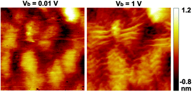
Metal–graphene interfaces generated by electrode deposition induce barriers or potential modulations influencing the electronic transport properties of graphene based devices. However, their impact on the local mechanical properties of graphene is much less studied. Here we show that graphene near a metallic interface can exhibit a set of ripples self-organized into domains whose topographic roughness is controlled by the tip bias of a scanning tunneling microscope. The reconstruction from topographic images of graphene bending energy maps sheds light on the local electro-mechanical response of graphene under STM imaging and unveils the role of the stress induced by the vicinity of the graphene–metal interface in the formation and the manipulation of these ripples. Since microscopic rippling is one of the important factors that limit charge carrier mobility in graphene, the control of rippling with a gate voltage may have important consequences in the conductance of graphene devices where transverse electric fields are created by contactless suspended gate electrodes. This opens up also the possibility to dynamically control the local morphology of graphene nanomembranes.


 Please wait while we load your content...