Indirect to direct band gap transition in ultra-thin silicon films†
Abstract
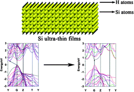
Free standing silicon layers undergo a transition from indirect to direct band gap semiconductor, which predicts a new possible way in silicon band gap engineering. The thickness and crystal orientation of the exposed surface are crucial. Our simulations reveal that the (100) films with thickness of ∼1.05 nm and (110) films with thickness of ∼1.14 nm could maintain the direct band gap structure. However, the (111) films always show indirect band gap structure even if the monolayer is constructed. The electron states density calculations were also carried out and the transition of the band gap structure is considered to be determined by the quantum confinement and surface termination conditions. The momentum


 Please wait while we load your content...