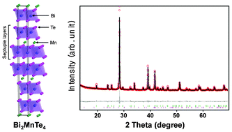
Crystal structure, properties and nanostructuring of a new layered chalcogenide semiconductor, Bi2MnTe4†
Abstract
A new layered chalcogenide semiconductor, Bi2MnTe4, was discovered. It was prepared by melting and

* Corresponding authors
a
Energy and Environmental Division, Korea Institute of Ceramic Engineering and Technology, 233-5 Gasan-dong, Geumcheon-gu, Seoul 153-801, Republic of Korea
E-mail:
yslim@kicet.re.kr
b Department of Materials Science and Engineering, Yonsei University, 134 Sinchon-dong, Seodaemun-gu, Seoul 129-749, Republic of Korea
c
LG Chem/Research Park, 104-1 Moonji-dong, Yuseong-gu, Daejeon 305-380, Republic of Korea
E-mail:
pmoka@lgchem.com
A new layered chalcogenide semiconductor, Bi2MnTe4, was discovered. It was prepared by melting and

 Please wait while we load your content...
Something went wrong. Try again?
D. S. Lee, T. Kim, C. Park, C. Chung, Y. S. Lim, W. Seo and H. Park, CrystEngComm, 2013, 15, 5532 DOI: 10.1039/C3CE40643A
To request permission to reproduce material from this article, please go to the Copyright Clearance Center request page.
If you are an author contributing to an RSC publication, you do not need to request permission provided correct acknowledgement is given.
If you are the author of this article, you do not need to request permission to reproduce figures and diagrams provided correct acknowledgement is given. If you want to reproduce the whole article in a third-party publication (excluding your thesis/dissertation for which permission is not required) please go to the Copyright Clearance Center request page.
Read more about how to correctly acknowledge RSC content.
 Fetching data from CrossRef.
This may take some time to load.
Loading related content
